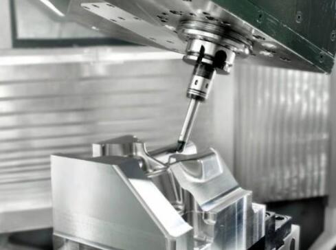
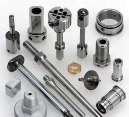
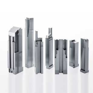
- Packaging materials and production process flow of semiconductor NC machining parts.
- What are the common semiconductor devices?
- New Packaging Materials for Semiconductor Devices and Their Classification
The semiconductor CNC machined parts
industry is one of the fastest growing industries in the world, which is widely used in aviation, aerospace, medical, automotive, electronics and other fields. Semiconductor packaging plays an important role in the development of semiconductor industry.
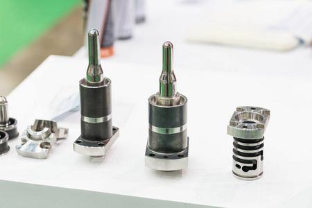
What are semiconductorThe semiconductor CNC machined parts?
Semiconductor The semiconductor CNC machined parts.
are a kind of materials whose conductivity is between metal conductors and insulators. The electronic devices with specific functions made of semiconductor materials are called semiconductor devices. Most semiconductor devices contain at least one PN junction formed by the contact between the P-type semiconductor region and the N-type semiconductor region. The characteristics and working process of semiconductor devices are closely related to this.
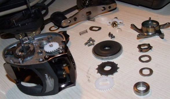
What are the common semiconductor devices?
We usually divide common semiconductors into four categories, as shown in the figure below, mainly including integrated circuits, discrete devices, sensors and optoelectronic devices.
The circuit made by integrating discrete devices on the substrate using a certain wiring and manufacturing process is called an integrated circuit. According to the different functions and structures of the circuit, it can be divided into analog circuit, microprocessor, logic circuit and memory. Sensors are used everywhere. Our common sensors include atmospheric monitoring sensors, smoke sensors in corridors and temperature sensors in cars. According to their application approaches and principles, they can be divided into physical sensors, chemical sensors and biological sensors; Optoelectronic devices mainly include optical devices, light receiving devices and optical composite devices, such as our common LEDs and OLEDs, optical fibers and some laser emitters, which belong to optoelectronic devices
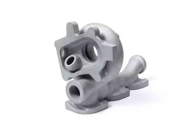
New Packaging Materials for Semiconductor Devices and Their Classification
There are mainly three types of common new semiconductor device packaging materials:
First, ceramic based packaging materials, which have the advantages of high mechanical strength, thermal stability, good air tightness and moisture resistance, play a strong role in protecting electronic systems, but have the disadvantage of high cost, and are suitable for packaging advanced microelectronic devices.
The other is plastic based packaging materials, which have the advantages of low material cost, simple process, small volume and light weight, while the disadvantages are high dielectric loss, high brittleness, mismatched thermal expansion coefficient and low thermal conductivity.
The third is metal based packaging materials, which have the advantages of high thermal conductivity and strength, but the disadvantages of high cost and are not suitable for large-scale industrialization.
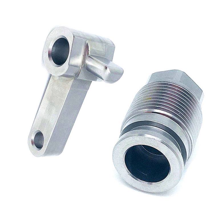
4、 Production process flow of The semiconductor CNC machined parts
The production process of semiconductor devices mainly consists of four parts, namely wafer manufacturing, wafer testing, chip packaging and post packaging testing.
Wafer manufacturing refers to the fabrication of circuits and electronic components on silicon wafers, such as transistors, capacitors, logic gates, etc. The whole process is complex, mainly including wafer cleaning, thermal oxidation, lithography (gluing, exposure, development), etching, ion implantation, diffusion, deposition, mechanical grinding and other steps to complete the processing and fabrication of circuits on wafers.
Wafer test refers to the wafer acceptance test of the electrical characteristics of the processed wafers. The purpose is to monitor the yield of the previous process and reduce the production cost.
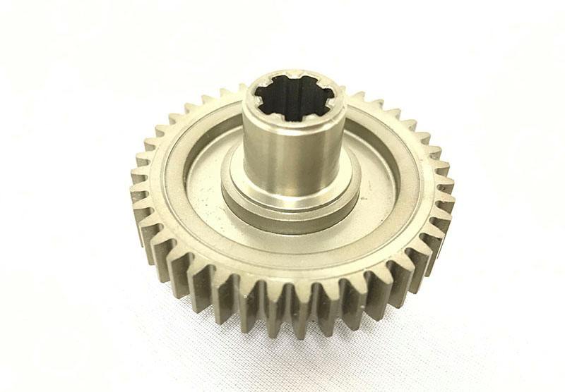
Chip packaging is the use of ceramic or plastic packaging crystals and wiring to form integrated circuits; It plays the role of fixing, sealing and protecting the circuit.
Post packaging test is to test the performance of the packaged chip to ensure the quality and performance of the device after packaging.

